From instant noodle packets to multimillion-dollar data centres, one Tokyo-based company has built a strange bridge between kitchen chemistry and cutting-edge semiconductors. Its near-monopoly on a thin insulating film now shapes the pace of progress in artificial intelligence.
From soup seasoning to the backbone of AI hardware
In Japan, Ajinomoto sits in supermarket aisles, not tech fairs. Most people associate the brand with stock cubes, instant ramen and flavour enhancers. Behind that familiar logo stands a diversified group worth billions, spanning food science, amino acids and high-performance chemicals.
The same expertise that once gave kitchens the savoury kick of umami now underpins the way modern processors are physically built. That shift did not happen by accident. It grew from a long history of tinkering with molecules and a talent for turning industrial leftovers into profitable materials.
A culinary breakthrough that set the tone
The company traces its roots to 1908. In Tokyo, chemistry professor Kikunae Ikeda became fascinated by the rich taste of his wife’s seaweed broth. It tasted neither salty, sweet, bitter nor sour. By isolating glutamate, he identified a fifth taste, later named umami.
Ikeda raced to commercialise this discovery. In 1909, he founded Ajinomoto, meaning “the essence of taste”. Early on, the firm focused on fermentation and food chemistry, producing seasonings on an industrial scale. Nobody at the time thought these skills would one day feed the semiconductor industry.
Ajinomoto’s deep experience in fermentation, amino acids and polymer chemistry created an unexpected launchpad for a critical electronics material.
Waste turned into a strategic material
When recycling became a winning bet
By the 1970s, Ajinomoto faced a very practical headache. Its processes for producing amino acids and flavour enhancers generated large volumes of chemical by-products. Treating or discarding them cost money and created regulatory pressure.
Instead of treating this output as pure waste, the research teams studied its behaviour. Some of the compounds showed strong electrical insulation, a stable response to heat and reliable mechanical properties. Not exactly a recipe, but promising raw material for something else.
For years, those characteristics sat without a clear market. That changed only in the 1990s, when chip manufacturers ran into a wall.
➡️ Klimakleber stoppen oder schützen
➡️ Wie ein windpark ein dorf zerreißt und aus klimafreunden erzfeinde macht
➡️ Warum deine angst vor kündigung dein größtes karriereproblem ist und du endlich aufhören musst dein eigener saboteur zu sein
➡️ Rentner muss landwirtschaftssteuer zahlen weil er wiese an imker verpachtet hat und keinen cent verdient
➡️ Schlechte nachrichten für weinliebhaber und winzer warum ein versteckter zuschlag auf jede flasche kommt und wie sich gastronomie verbraucher und politiker darüber zerstreiten
➡️ The future “world’s largest aircraft” just signed a heavyweight alliance that could clear its runway to commercial success
➡️ Familie soll ihr Gemüse im Vorgarten entfernen, warum der Fall den ganzen Ort spaltet
➡️ Schlechte nachrichten für rentner mit nebenjob in landwirtschaft und imkerei sie sollen plötzlich steuern zahlen und fühlen sich enteignet
Intel hits the miniaturisation ceiling
By 1996, Intel and other leading players in Silicon Valley were pushing transistor sizes down and clock speeds up. As more circuitry crammed into the same space, old approaches to insulating and connecting layers began to fail.
Traditional insulating inks used on chip substrates struggled. They trapped air bubbles, dried unevenly and sometimes contaminated delicate structures. Yields suffered. At the tiny scales involved, a few defects meant whole batches of high-end chips had to be scrapped.
Somewhere in Intel’s supplier network, a question popped up: could a continuous insulating film, rather than a liquid ink, fix this?
Engineers wanted a clean, uniform film they could laminate, drill and pattern with near-microscopic precision.
Four months that changed chip packaging
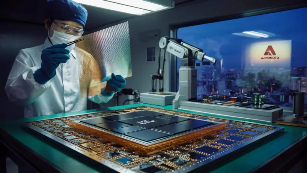
Ajinomoto took on the challenge. In just a few months, its chemists and materials engineers engineered a new film based on epoxy resins and filler materials tuned for electronics.
This product, later named Ajinomoto Build-up Film (ABF), looked nothing like instant soup powder. It formed an ultra-thin, smooth sheet that could be applied to a substrate, heated, and then drilled or etched to form tiny channels for copper wiring.
- It withstands temperatures above roughly 200°C without degrading.
- It can be patterned with lasers at micrometre scales while keeping its shape.
- It supports dense copper interconnects between chip and circuit board.
- It maintains strong insulation even as wiring distances shrink.
Each new chip generation pushed ABF further. Ajinomoto had to tweak thickness, chemistry and thermal response constantly, in lockstep with the cutting-edge packaging tools used at foundries such as TSMC.
How Ajinomoto ended up with 95% of a global market
From Intel to almost every advanced chip
Intel officially adopted ABF for high-end products in 1999. Others followed. AMD, Broadcom, Qualcomm and many more began to rely on ABF-based substrates for complex processors.
Today, almost every powerful CPU or GPU that sits in servers, PCs, games consoles or advanced networking hardware uses substrates incorporating ABF. The material sits buried under layers of silicon and solder, invisible to consumers, yet absolutely central to performance.
Without ABF, a cutting-edge chip may exist on silicon, but it cannot be practically wired into a usable product.
Because the formula is tricky to reproduce and requires years of tuning with each customer, Ajinomoto has kept an extraordinary grip on the market. Industry analysts estimate the company supplies more than 95% of the global demand for build-up films of this kind.
| Stage | Year | Impact on ABF |
|---|---|---|
| Umami discovery and company founding | 1908–1909 | Builds core know-how in amino acids and food chemistry |
| Study of by-products | 1970s | Identifies insulating, heat-resistant materials |
| Intel packaging crisis | Mid-1990s | Triggers development request for a new film |
| ABF adoption in high-end processors | Late 1990s–2000s | ABF becomes an industry standard for substrates |
| AI boom and advanced packaging | 2020s | Demand for ABF accelerates with massive GPUs and AI accelerators |
The hidden link between Ajinomoto and Nvidia’s AI accelerators
Why AI chips need exotic packaging
Modern AI accelerators, such as Nvidia’s latest GPUs, no longer operate as single slabs of silicon. They are vast assemblies. Logic dies, stacks of high-bandwidth memory (HBM) and sometimes interposers all sit together in one tightly integrated package.
To build that package, Nvidia relies heavily on TSMC’s advanced packaging technology known as CoWoS, short for chip-on-wafer-on-substrate. In this process, chips and memory are mounted on an intermediary layer before the whole structure meets the circuit board.
That intermediary layer, the substrate, behaves like a miniature, extremely dense circuit board. It must handle thousands of data lines, withstand challenging thermal loads and remain dimensionally stable across temperature swings. ABF sits at the core of this substrate stack.
Every high-end Nvidia GPU used for training large AI models relies on ABF-based substrates produced in Japan.
Even as Nvidia and others talk about “agentic” AI and multi-step reasoning, the physical constraints remain brutal. Without a material like ABF to link chips to memory at high speed and high density, those AI models would run far slower or not at all at current scales.
When one film slows the whole industry
The 2021–2022 global chip shortage made this dependency very visible. While headlines focused on missing car chips or game consoles, a quieter crunch hit high-performance components. Lead times for certain networking and custom chips from companies such as Broadcom stretched well past a year.
One reason sat far from the spotlight: limited supply of ABF. Even if a foundry had enough silicon wafers and lithography tools, it could not ship finished products without the right substrates. Capacity for ABF could not be expanded overnight. Facilities need specialised equipment, tight quality controls and close integration with customer processes.
The situation highlighted a fragile point: a single mid-layer material, made mostly in one country by one firm, can become a brake on global computing progress.
Rising AI demand and what comes next
Growth powered by data centres, not dinner tables
Ajinomoto still sells seasonings by the ton, but the growth story now leans heavily on data centres. The company has announced ambitious plans to boost ABF production capacity by roughly half by the end of the decade. Industry forecasts point to annual demand growth of around 8–10%.
Each new AI accelerator chip eats more substrate area. More memory stacks, wider buses, power delivery networks and signal integrity constraints all require extra layers of ABF-based film. So even if the number of chips stayed flat, the surface area of ABF per chip keeps climbing.
As long as AI workloads scale, Ajinomoto’s electronic materials arm should track that rise almost automatically.
Key terms that shape the stakes
A few technical concepts help clarify why this single material matters so much:
- Substrate: The multi-layer base on which the chip package sits, routing signals and power between the silicon die and the circuit board.
- Packaging: The stage where bare chips are mounted, wired, protected and connected. It often decides how fast a device can communicate and how much heat it survives.
- HBM (high-bandwidth memory): Memory stacked vertically close to the processor, delivering massive data rates needed for AI workloads.
- ABF: An epoxy-based insulating film built up in layers inside the substrate to separate and guide high-density copper wiring.
If any of these parts falter, performance drops or costs spike. In that sense, Ajinomoto’s film sits on the same strategic plane as advanced lithography machines or top-end GPU designs, even if its price tag per unit looks modest.
Risks, rivals and possible scenarios
Ajinomoto’s dominant position brings several risks for the wider industry. Geopolitical tensions, earthquakes, supply chain disruptions or quality issues at a handful of factories could ripple into delayed AI system rollouts worldwide. Chipmakers quietly factor that into their contingency planning.
Rivals in the US, Europe, Taiwan and mainland China aim to develop alternatives, often with governmental backing as part of broader “chip sovereignty” strategies. Yet replicating decades of tacit knowledge — from polymer mixtures to process tuning — will take time. Early substitutes may work for simpler chips, but struggle with the extreme density and reliability standards of top-tier AI GPUs.
One plausible scenario sees Ajinomoto remain the reference supplier for the most advanced nodes, while regional competitors win share in mid-range or legacy packaging. Another path might shift some of the pressure away if chip designs move towards chiplets or optical interconnects that lean less on current substrate architectures.
For now, though, every new wave of AI, from recommendation engines to generative models and agentic systems, rests partly on a quiet Japanese success story that began with a bowl of seaweed soup and ended in the racks of hyperscale data centres.